Top 2023 Automation Trends for Wafer Handling Solutions
IT Administration
June 20, 2023

Semiconductor manufacturers face the challenge of creating new and more efficient ways of handling their wafers. With the range of shapes and sizes, they each require unique handling requirements. To achieve this, the industry must continue pursuing and adopting new technologies that increase process effectiveness and environmental requirements.
There was a great deal of media coverage as the knock-on effect of the chip shortage impacted the general public. However, despite immense investment and support for the semiconductor industry, 2022 was a volatile year.
The future of the industry is conflicted. Despite the belief that the global semiconductor market revenue will shrink by four percent in 2023, innovations in electronics and semiconductor manufacturing are critical drivers for the global wafer handling robot market.
According to a senior research analyst at Technavio, “… there will be an increase in the demand for wafer handling robots because they possess positioning capabilities and can operate efficiently to ensure micrometer-scale accuracies and tolerances. There is also an increase in the demand for vacuum wafer handling robots for the fabrication of ICs under vacuum conditions as these conditions ensure that the particulates can be controlled and there is minimal contamination.”
What wafer handling trends does 2023 have in store for the semiconductor industry?
We are well into 2023, and regardless of what happens to global revenue in our industry, we need to work together as a collective group and help direct the best path forward. Consider the following significant trends that we see shaping our industry today and into the future –
– Impact of Artificial Intelligence on Robotic Development
The rise of AI solutions is forcing semiconductor companies to integrate Artificial Intelligence into manufacturing workflows to optimize operations and increase efficiencies. AI and machine learning are changing the landscape of how we operate. Robots will continue to push the boundaries of precision engineering. It’s important to embrace those challenges to push improvements and innovation.
– Cleanliness and Particle Contamination Control
Contamination control in a semiconductor fab is critical. Particles, gels, metals, and airborne molecular contaminates damage products, processes, and equipment. A detection system can recognize possible contamination, identify its sources, and generate an alert for additional cleaning procedures. Additionally, a system with unidirectional airflow can keep airborne particles from settling on contamination-sensitive products. With wafers, studies show the effects of static charge represent a substantially greater contamination source than that of sedimentation.
– Smart Predictive Maintenance
To perform at the highest levels, it’s about testing and predictability. A robot failure can force unplanned downtime and the loss of production. Predictive maintenance of robots can increase productivity and cut costs in highly automated production systems. There are tremendous benefits when you can proactively detect changes in machine vibration and friction and provide an advanced warning before a failure.
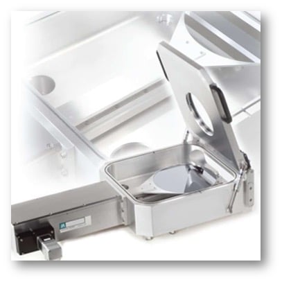
– 200mm vs. 300mm Wafer
The number of semiconductor fabs using 300mm wafers continues to increase. The manufacturing cost-benefits of processing chips on sizable wafers play a considerable role. Larger wafers address the challenges that companies face daily to reduce the size of electronic devices while lowering costs and maintaining high quality.
– Shift to U.S. Semiconductor Research and Development (R&D)
R&D is critical for the country to move forward and continue being seen as a technology leader. To support innovation, the U.S. semiconductor industry invested $50 billion in R&D in 2021. Furthermore, with the passage of the CHIPS and Science Act, the federal government is set to make its single largest investment in semiconductor R&D ever, strengthening our U.S. technological competitiveness.
– Chips Act / U.S. Security of Designs
According to the Congressional Research Service (CRS), the United States’ share of global semiconductor fabrication capacity has been on a steady decline for years, falling from approximately 45 percent in 1990 to around 12 percent in 2020. The Act provides financial assistance, $52 billion, for chip manufacturing incentives and research investments, as well as an investment tax credit for semiconductor manufacturing and semiconductor equipment manufacturing. Ideally, these investments will reinvigorate the U.S. and reinforce the economy, national security, and supply chains.
It’s an exciting time to be in the semiconductor industry as we watch these trends play out in an increasingly competitive environment. Looking ahead, we are confident that we will be able to react quickly to customer needs and improve experiences continuously and in real-time.
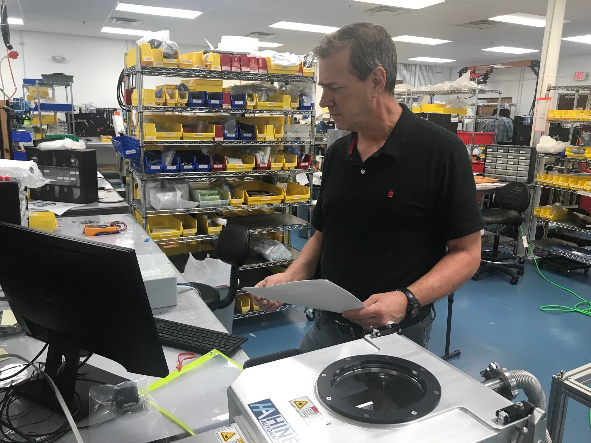
About Hine Automation
From initial concept to design to delivery, Hine builds and automates with precision and passion. Its team has been developing robotic and automated wafer handling solutions for more than 30 years. Contact us today or visit us at HineAutomation.com to learn more.